

The Traitorous 8 and Birth of Silicon Valley
Courtesy of Wade of Investing Caffeine
Over my 25 year investment career, I’ve made quite a few technology investments and visited dozens of Silicon Valley companies. I heard bits and pieces about the story of the Traitorous 8, but I never fully comprehended the technology revolution they started. Out of intellectual curiosity, I decided to delve a little deeper into the topic.
At the heart of this topic is a small device about the size of a fingernail. This object has several different names and can be quite confusing. The official name is an integrated circuit or IC, but usually it’s referred to as a chip, microchip, or semiconductor. These chips have become ubiquitous, scattered invisibly throughout our daily lives in our cars, computers, TVs, cell phones, appliances, and remote controls (an average household is home to about 1,000 of these semiconductors). Despite most people taking the microchip for granted, this diminutive piece of silicon created from our beach’s sand have contributed the largest burst of wealth creation in human history.
Before gaining a true understanding into the birth of Silicon Valley, we have to better understand the historical context in which the global technology capital was created – this takes us back to the early twentieth century when the vacuum tube was inventedin 1904. Before Al Gore invented the Internet, we needed computers, and before we had personal computers, we needed integrated circuits, and before we had integrated circuits we had vacuum tubes (see chart below). Vacuum tubes were the electronic circuitry components required to make telephones, radios and televisions work in the early 1900s.
Tech History & the Vacuum Tube
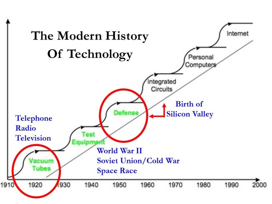
The vacuum tube was invented in 1904 by an English physicist named John Ambrose Fleming. Like semiconductors, the main function of a Vacuum tube is to control the flow of electric current. More specifically, a vacuum tube controls the current transferred between cathode and anode to make a circuit. Vacuum tubes were used for amazing applications, but in modern society this technology has been largely replaced by semiconductors, primarily because of cost, scalability and reliability factors.
The first all-electronic digital computer title is usually awarded to the ENIAC computer, which stood for Electronic Numerical Integrator and Calculator. ENIAC was built at the University of Pennsylvania between 1943 and 1945 by two professors, John Mauchly and J. Presper Eckert. World War II, the Soviet Union Cold War, and the space race kicked off by the Sputnik launch all pushed the vacuum tube technology to its limits. To give you an idea of how costly and inefficient vacuum tubes were relative to today’s microchips consider some of the ENIAC statistics. ENIAC filled a 20 x 40 foot room; weighed 30 tons; used more than 18,000 vacuum tubes; and only operated 50% of the time because operators were continuously replacing burned out vacuum tubes. In fact, the ENIAC vacuum tubes generated so much heat, the temperature in the computer room often reached 120 degrees.
Shockley – The Godfather of the Transistor
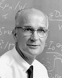
Something had to change to improve vacuum tube technology, and it did…thanks in large part to a physicist named William Shockley, the so-called “Godfather of the Transistor.” Shockley received his Bachelor of Science degree from Caltech in 1932 and earned his Ph.D. degree from MIT in 1936. After graduation, Shockley left the famous Bell Labs research center, which was a research division of AT&T at the time (now owned by Nokia). As part of Shockley’s work at Bell Labs in the late 1940s, he contributed to the invention of the transistor with experimentalist Walter Brattain and quantum theorist John Bardeen. Fundamentally, the transistor is a switch, which over time has shrunk down to the size of a virus. The transistor is what ultimately replaced the vacuum tubes because it is smaller, more efficient, more reliable, more durable, and cheaper than vacuum tubes. Transistors switch and amplify the flow of electronic signals to create digital ones and zeros that instruct electronic applications. Without the benefits of shrinking transistors, today’s computer servers would be three stories high.
How small have transistors become? Take the iPhone 6 for example – it uses the A8 chip, which is made up of a whopping two billion transistors. To accomplish this feat, engineers are now creating transistors at the atomic level. Large semiconductor manufacturers like Intel Corp (INTC) are now developing transistors at the 10 nanometer level. To put this scale into perspective, consider a sheet of paper is approximately 100,000 nanometers thick. So in order to create a 10 nanometer sheet of paper, one would have to slice a single sheet 10,000 times thinner to reach 10 nanometers…mind-boggling.
Building atomic sized transistor technology is very cool, but also very expensive. Only a handful of semiconductor manufacturers have enough capital to build these new state-of-the art facilities. Case in point is Intel’s D1X fabrication facility in Hillsboro, Oregon, which is estimated to have cost $6 billion. Like seeing the pyramids – it’s difficult to understand the enormity of the structure without visiting it, which I was fortunate to do in 2014. It’s very ironic that in order to build these microscopic transistors and integrated circuits, multi-billion dollar manufacturing facilities the size of 38 football fields (~2.2 million square feet) are required. Another example of a next-generation manufacturing facility is Taiwan Semiconductor’s – Fab 15 (TSM), which was estimated to cost $9.3 billion.
These mega-transistor manufacturing facilities would not have been possible without Shockley’s contributions. Having helped invent the transistor largely replace the dominant computing technology of the last half century (i.e., vacuum tube), Shockley mustered up the courage to leave Bell Labs and start his own company, but he needed some cash to make it happen. He contacted Arnold Beckman, CEO of Beckman Coulter and his old professor at Caltech. Over a boat ride in Newport Beach, California, Shockley asked Beckman for $1 million to start his own lab. Silicon Valley potentially could have started in Southern California, but Shockley explained his aging mother lived in Palo Alto and convinced Beckman to start Shockley Semiconductor Laboratory in Mountain View, California during 1956.
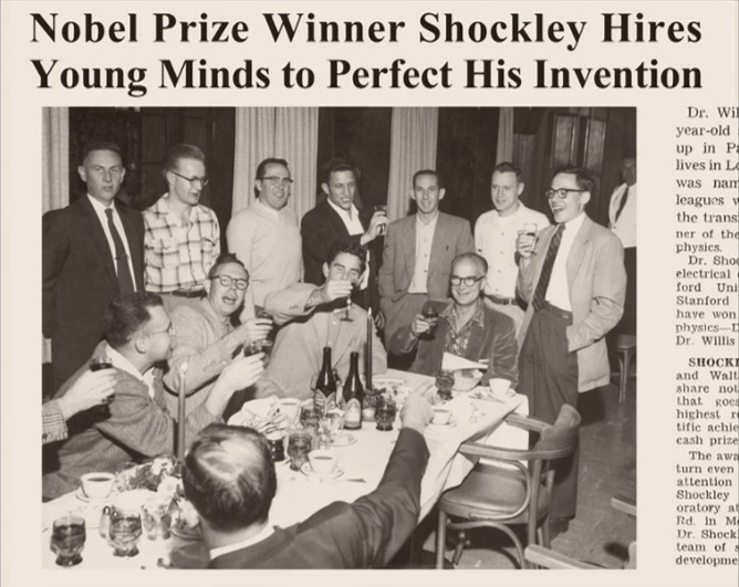
After Shockley Semiconductor began operations, everything appeared to be going according to plan. Shortly after opening shop and recruiting the best and brightest engineers across the country, Shockley and his former Bell Labs colleagues Walter Brattain and John Bardeen were notified they all had won the Nobel Prize in physics (see photo below).
After the Nobel Prize celebrations, everything went downhill quickly. Shockley was known as a brilliant engineer but a horrific manager. He put his employees through a battery of tests including psychological tests, intelligence tests, and even lie detector tests. Shockley also posted employee salaries publicly and recorded phone calls. He was a paranoid individual who believed his workers were stealing trade secrets and sabotaging projects, so therefore he wouldn’t share findings with his research staff. Adding insult to injury, Shockley was a racist, who believed blacks were genetically inferior with subpar IQs, so they shouldn’t have kids.
Here is a video link summarizing William Shockley’s leadership:
The Traitorous 8 Surface
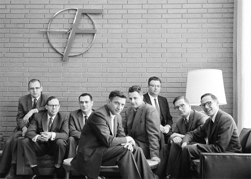
In 1957, the year after Shockley Semiconductor Labs started up, the division reached 30 employees. Eight of the employees, Sheldon Roberts, Eugene Kleiner, Victor Grinich, Jay Last, Julius Blank, Jean Hoerni, Robert Noyce, and Gordon Moore finally said, enough-is-enough and decided mutiny was their best option.

The disgruntled group ended up contacting a 30-year-old, snot-nosed, Harvard MBA graduate named Arthur Rock, the individual who eventually coined the phrase “venture capitalist.” In 1957, Rock was a New York banker working at Hayden Stone & Co. Rock believed the group of eight engineers (six of which had Ph.Ds) deserved attention, given their experience working with a Nobel Prize winner. The Traitorous 8 simply wanted to find an employer that would hire them as a group, but Rock advised them to start their own company – a novel idea during the 1950s.
After making a list and calling about 40 blue chip companies from the Wall Street Journal for funding, Rock almost gave up until they received a lead to contact Sherman Fairchild. Fairchild was a wealthy entrepreneur and playboy who hung out at the El Morocco in New York with Howard Hughes. Rock convinced Fairchild, the CEO of Fairchild Camera & Instrument, to invest $1.5 million into a Traitorous 8 startup.
The rest is history. The Traitorous 8 set up shop as Fairchild Semiconductor (FCS) in Mountain View, about twelve blocks from Shockley’s operations. Over the next 10 years, Fairchild Semiconductor grew from twelve employees to twelve thousand employees, and raked in some $130 million in annual revenues. Of the original Traitorous 8, two have become historical figures – Robert “Bob” Noyce and Gordon Moore. All good things come to an end, and Noyce and Moore increasingly got frustrated with Fairchild’s mismanagement of the semiconductor division.
After Fairchild passed over Noyce for a CEO promotion in 1968, Noyce told Moore, “I’m going to leave, are you interested?” Moore agreed, so he and Noyce contacted Arthur Rock again for his assistance. Rock quickly helped them raise $2.5 million, and Intel Corporation (short for “Integrated Electronics”) was born. Three years later in 1971, Intel launched its IPO at $23.50 per share ($.02 split-adjusted). An investment of $10,000 back then would be worth about $12,000,000 today –about a +120,000% return.
Here’s a video summarizing the creation of Intel:
Thomas Edison of Silicon Valley
Nowadays, Noyce is hailed by many as the “Thomas Edison of Silicon Valley.” Noyce received his Ph.D. from MIT and is most known for his invention of the integrated circuit. During the late 1950s, other engineers also worked on the IC, including Jack Kilby at Texas Instruments, but Noyce received the first patent in 1961. Unlike Kilby, who created his IC from germanium, Noyce created his IC from silicon, the semiconductor of choice still today. After a decade of litigation, Noyce and Kilby settled their differences and decided to cross-license their patents. Unfortunately, the Nobel Foundation doesn’t issue Nobel Prizes posthumously, so when the Nobel Prize was issued for the invention of the integrated circuit in the year 2000 (10 years after Noyce’s death), only Kilby was recognized. To Kilby’s credit, he acknowledged the contributions of Noyce and others in his Nobel speech with a story of a rabbit and beaver looking up at the Hoover Dam, “No, I didn’t build it myself. But it’s based on an idea of mine!”
Moore’s Law Established
Arguably, Moore was just as influential as Noyce, but due to his quiet leadership style, Moore is often overlooked. Moore was a year younger than Noyce and earned his chemistry degree from Berkeley and Ph.D. from Caltech. Unlike Noyce, who grew up in the Midwest (Iowa), Moore was raised near Palo Alto, which made recruiting Moore by William Shockley quite easy. Moore’s largest contribution is considered to “Moore’s Law,” which generally states the number of transistors (i.e., a chip’s computing power) will double every 1-2 years. During the 1980s, Noyce described the implications of Moore’s Law by comparing Moore’s Law to the airline industry. If the airline industry progressed at the trajectory of the semiconductor industry over the last 20 years, then the 767 airplane would cost $500 and travel around the world in 20 minutes on five gallons of gas. Regrettably, not many industries advance at the pace of semiconductors.
Moore came up with “Moore’s Law” when her wrote a seminal article for Electronics magazine in 1965 and in the article he properly predicted that the number of transistors that could be squeezed onto a microchip (around 60 at the time) would increase 1,000-fold to 60,000 transistors by 1975. It would take decades for his projections to come true, but Moore very presciently predicted the explosion of home computers, cell phones (which he called “portable communications equipment”), electronic wrist-watches, digital cars, and a host of other electronic devices and applications. A half century later, Moore’s Law holds true, but the pace of transistor growth admittedly is slowing. The physics behind semiconductor manufacturing is running into serious limitations of quantum mechanics, cost, and heat. Microchips are becoming so dense and fast that the internal components in many cases are melting the chips in research labs.
Here is a video link summarizing Moore’s Law:
While Moore’s Law is approaching diminishing returns, the costs of microchips keep declining, power keeps increasing, and efficiency keeps improving. Despite the slowing in Moore’s Law, as you can see below, the adoption of transistors via microchips is not plateauing. According to Intel, we are now consuming an estimated sextillion transistors!
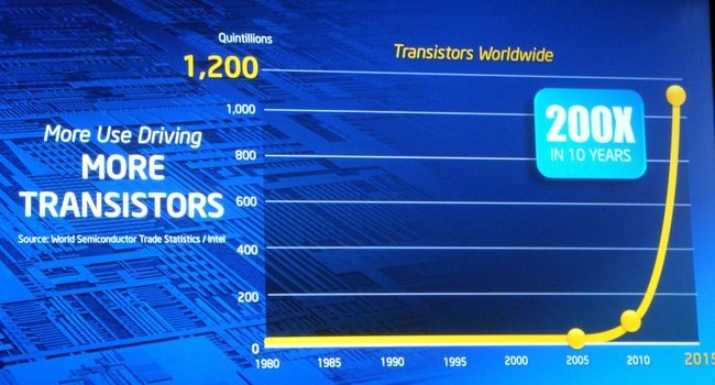
Source: Intel Corporation
Politics, economics, terrorism, and social issues may dominate the daily headlines, but behind the scenes there are daily miracles occurring due to technology advancements. Driving much of that innovation is the microchip, and without the Traitorous 8, the world would look a lot different and there would be no Silicon Valley as we know it today. Had Robert Noyce and Gordon Moore miserably resigned themselves to remain at Shockley Semiconductor, perhaps mankind would not have achieved the giant strides in global standards of living (see chart below). Thankfully, their contributions live on today and ensure a bright future for our kids, grandchildren, and the world at large.
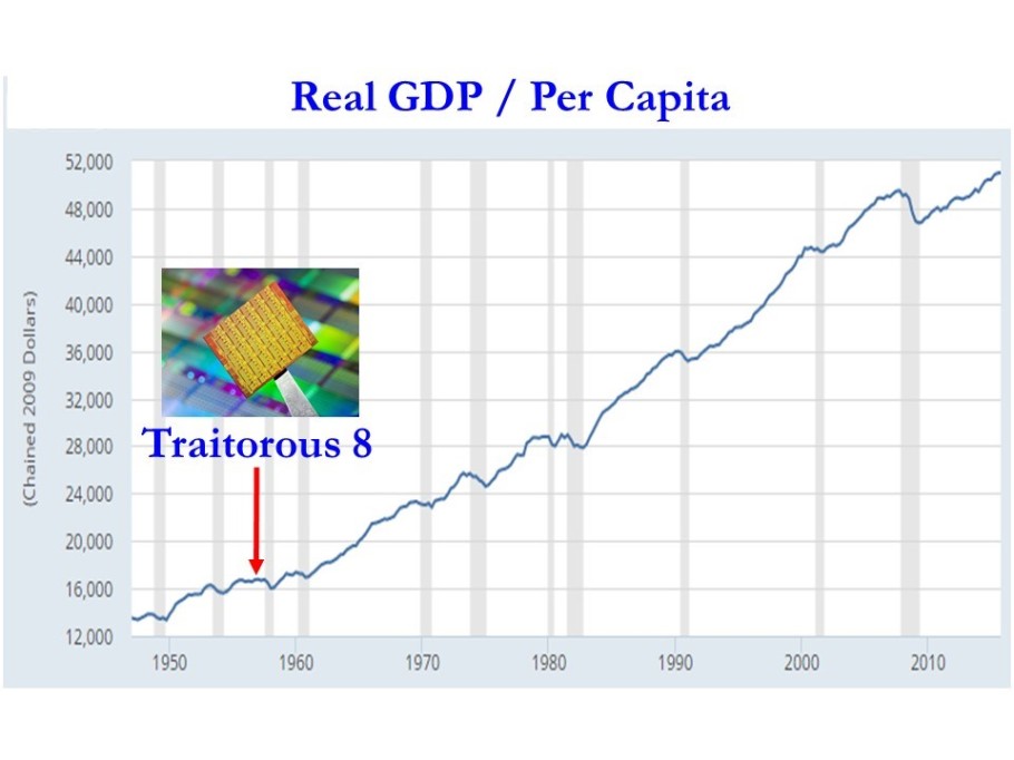
Source: FRED
Wade W. Slome, CFA, CFP®
Plan. Invest. Prosper.
DISCLOSURE: Sidoxia Capital Management (SCM) and some of its clients hold positions in certain exchange traded funds (ETFs) and in INTC (non-discretionary), TXN (non-discretionary), T (non-discretionary), but at the time of publishing had no direct position in TSM, NOK, FCS, or any other security referenced in this article. No information accessed through the Investing Caffeine (IC) website constitutes investment, financial, legal, tax or other advice nor is to be relied on in making an investment or other decision.